🖥️
Chapter 1.1 — Basic Functional Units
🖥️ CHAPTER 1.1 — BASIC FUNCTIONAL UNITS MIND MAP
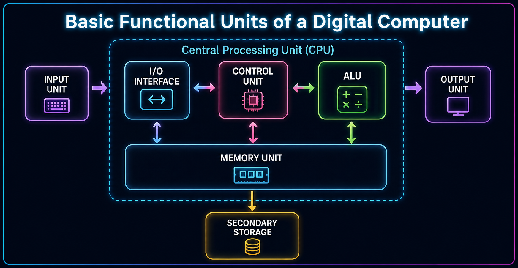
5 Units → Input, Memory, ALU, Control Unit, Output (ALU + CU + Registers = CPU)
Registers → PC (next instr), IR (current instr), MAR (address), MDR (data), AC, GPRs
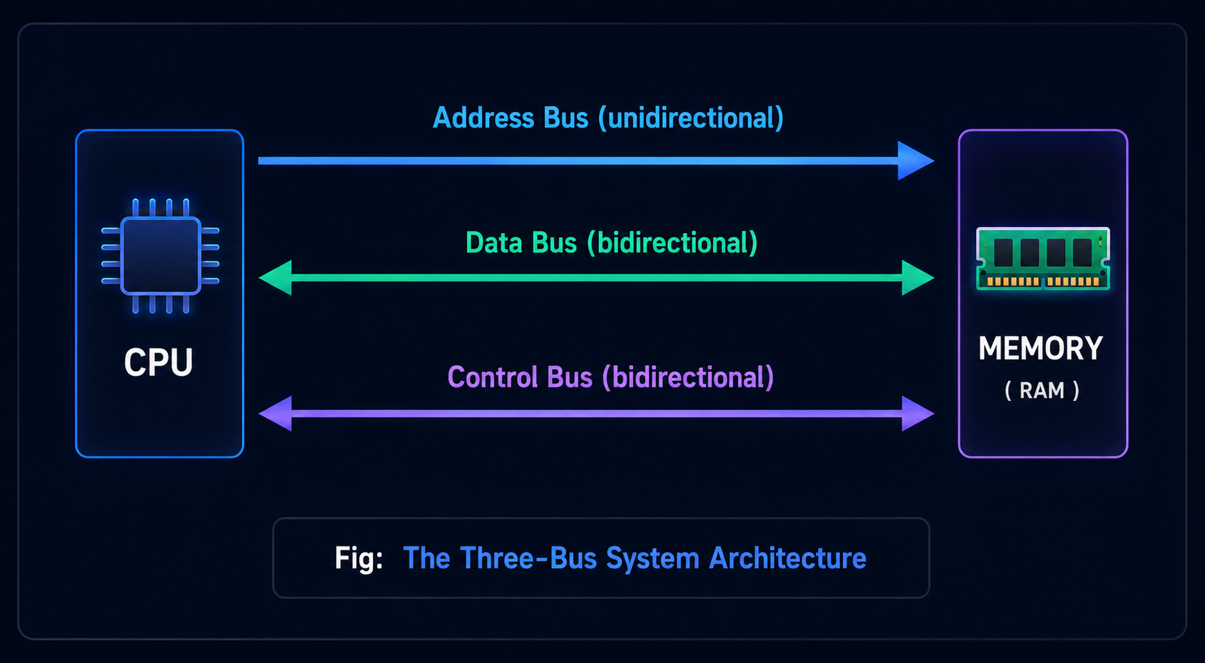
3 Buses → Address (one-way), Data (two-way), Control (two-way, signals)
I/O Addressing → Memory-Mapped (shared space) vs Isolated (separate space, IN/OUT)
1. Digital Computer and its Components
📖 Digital Computer: An electronic device that processes data in binary (0s and 1s) form by accepting input, performing arithmetic/logical operations, and producing output — all under the control of stored instructions (a program).
Five Basic Functional Units:
🖥️ Basic Functional Units of a Digital Computer
| Unit | Function |
|---|
| Input Unit | Accepts data/instructions from the outside world (keyboard, mouse, scanner) and converts them into binary form |
| Memory Unit | Stores data and instructions, both before processing and after (Primary — RAM/ROM, Secondary — Hard disk) |
| ALU (Arithmetic Logic Unit) | Performs all arithmetic (add, subtract) and logical (AND, OR, comparison) operations |
| Control Unit | Directs and coordinates all other units — fetches instructions, decodes them, and generates control signals |
| Output Unit | Converts processed binary results back into human-readable form (monitor, printer) |
💡 CPU = ALU + Control Unit + Registers. Together with Memory and I/O units, these five form the complete computer system — this classification is a very common 2-mark question.
2. Computer Registers
📖 Register: A small, extremely fast storage location built directly into the CPU, used to hold data, addresses, or instructions temporarily during processing. Registers are the fastest form of memory in the entire system.
| Register | Full Form | Purpose |
|---|
| PC | Program Counter | Holds the address of the next instruction to be fetched |
| IR | Instruction Register | Holds the instruction currently being executed |
| MAR | Memory Address Register | Holds the address of the memory location to be accessed (read/write) |
| MDR / MBR | Memory Data/Buffer Register | Holds the data being transferred to/from memory |
| AC | Accumulator | General-purpose register that holds intermediate arithmetic/logic results |
| GPRs | General Purpose Registers | Multiple registers (R0, R1, R2...) used to hold temporary data/operands for the CPU |
| SP | Stack Pointer | Points to the top of the stack in memory |
| PSW / Flags | Program Status Word | Holds condition flags — Carry, Zero, Sign, Overflow — set after ALU operations |
💡 How they work together (fetch example):
1. PC holds address 200 → copied into MAR
2. CPU reads memory at that address → instruction lands in MDR
3. Instruction moves from MDR → IR for decoding
4. PC increments to 201 (next instruction)
💡 Exam Tip: PC vs MAR is a classic confusion — PC always points to the next instruction's address; MAR holds the address currently being accessed in memory (could be for data too, not just instructions).
3. System Bus Structure — Data, Address & Control Bus
📖 Bus: A shared group of parallel wires that carries information between the CPU, memory, and I/O devices. Instead of separate dedicated wires between every component, a bus lets everything share one common highway.
🚌 Three Bus System Architecture
| Bus Type | Direction | Carries |
|---|
| Address Bus | Unidirectional (CPU → Memory/IO) | The memory address CPU wants to read from / write to. Width decides max addressable memory (n-bit bus → 2ⁿ locations) |
| Data Bus | Bidirectional | The actual data being transferred. Width decides how many bits moved per cycle (e.g. 32-bit or 64-bit bus) |
| Control Bus | Bidirectional | Control signals — Read, Write, Memory/IO select, Clock, Interrupt, Ready/Busy |
Formula: Maximum Addressable Memory = 2^(address bus width)
Example: 32-bit address bus → 2³² = 4,294,967,296 locations = 4 GB max memory
Worked Example — Reverse Calculation:
💡 Q: How many address lines are needed to address 1 MB of memory?
1 MB = 2²⁰ bytes (1 MB = 1024 × 1024 bytes = 2¹⁰ × 2¹⁰ = 2²⁰)
We need 2ⁿ ≥ 2²⁰ → so n = 20 address lines
Q: How many address lines for 4096 memory locations?
4096 = 2¹² → n = 12 address lines
💡 Exam Tip: Address Bus is one-way (CPU tells memory WHERE), Data Bus is two-way (data flows in both directions — CPU can read from or write to memory). This direction difference is a favourite 2-mark question. For numericals, remember: number of address lines = log₂(memory size in locations).
4. Overview of Memory and I/O Addressing
📖 Addressing: The method the CPU uses to identify and access a specific memory location or I/O device using a unique address.
Memory Addressing:
Every memory location has a unique address, starting from 0 up to (Memory Size − 1). The CPU places the required address on the Address Bus, and the Control Bus signals whether it's a Read or Write operation.
Primary Memory vs Secondary Memory:
📖 Primary Memory (Main Memory): Memory directly accessible by the CPU — volatile, very fast, but limited in size and expensive per byte. Examples: RAM, Cache, Registers.
📖 Secondary Memory (Auxiliary/Storage Memory): Memory NOT directly accessible by the CPU — data must first be loaded into primary memory before the CPU can use it. Non-volatile, slower, but much larger capacity and cheaper per byte. Examples: Hard Disk, SSD, Pen Drive, CD/DVD.
| Feature | Primary Memory | Secondary Memory |
|---|
| CPU Access | Direct | Indirect (via primary memory) |
| Volatility | Volatile (data lost on power-off) — except ROM | Non-volatile (data persists) |
| Speed | Very fast | Much slower |
| Capacity | Small (GBs) | Large (TBs) |
| Cost per Byte | Expensive | Cheap |
| Examples | RAM, Cache, Registers | Hard Disk, SSD, DVD, Pen Drive |
💡 Exam Tip: The core distinguishing test: "Can the CPU directly execute instructions/data from it, or must it be copied into RAM first?" — Primary = direct access, Secondary = always needs to be loaded into Primary first.
I/O Addressing — Two Methods:
| Method | How it Works | Example |
|---|
| Memory-Mapped I/O | I/O devices share the SAME address space as memory. Same instructions (MOV, LOAD) used for both memory and I/O | ARM processors |
| Isolated (I/O-Mapped) I/O | I/O devices have a SEPARATE address space from memory. Needs special instructions (IN, OUT) | Intel x86 processors |
✅ Memory-Mapped I/O Advantage: Simpler — any memory-referencing instruction works on I/O too, no special instructions needed.
❌ Memory-Mapped I/O Disadvantage: Reduces the memory address space available for actual memory, since I/O devices "eat into" the same address range.
💡 Exam Tip: "Memory-mapped vs Isolated I/O" comparison is a very common 5-mark differentiate question — remember: shared space vs separate space, and generic instructions vs special instructions (IN/OUT).
🔢
Chapter 1.2 — Data Representation
🔢 CHAPTER 1.2 — DATA REPRESENTATION MIND MAP
Fixed-Point → Signed Magnitude, 1's Complement, 2's Complement (preferred — one zero, simple HW)
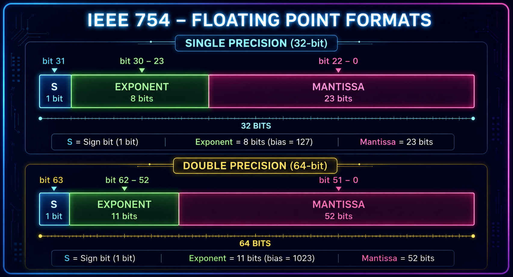
Floating-Point (IEEE 754) → Sign + Exponent(biased) + Mantissa; Single=32-bit, Double=64-bit
Add/Sub → 2's complement turns subtraction into addition; overflow = same-sign inputs, opposite-sign result
Multiplication → Array Multiplier (shift-add) vs Booth's Algorithm (skips 0/1 runs, handles signed numbers)
1. Fixed-Point Number Representation
📖 Fixed-Point Representation: A way of representing numbers (mainly integers) in binary where the position of the binary/decimal point is fixed — used for representing signed numbers in a computer.
| Method | Rule | +9 in 8-bit | -9 in 8-bit |
|---|
| Signed Magnitude | MSB = sign (0=+, 1=-), remaining bits = magnitude | 0000 1001 | 1000 1001 |
| 1's Complement | Negative = flip all bits of positive number | 0000 1001 | 1111 0110 |
| 2's Complement | Negative = 1's complement + 1 | 0000 1001 | 1111 0111 |
Worked Example — Represent -45 in 8-bit:
💡 Step-by-step conversion:
Step 1: Write +45 in binary (8-bit) → 0010 1101
Step 2 (Signed Magnitude): Flip only the MSB to 1 → 1010 1101
Step 3 (1's Complement): Flip ALL bits of +45 → 1101 0010
Step 4 (2's Complement): Take 1's complement, then add 1 →
1101 0010 (1's complement) + 1 = 1101 0011
💡 Verify (2's Complement): To check, take 2's complement of the result again — you should get back +45. 1101 0011 → flip bits → 0010 1100 → +1 → 0010 1101 = 45 ✓
Why 2's Complement is Preferred:
✅ Only ONE representation of Zero (Signed magnitude & 1's complement have +0 and -0 — wastes a bit pattern)
✅ Simpler hardware — subtraction is done using the same adder circuit as addition (no separate subtractor needed)
✅ No special end-around carry handling needed (unlike 1's complement)
| Range (n-bit) | Signed Magnitude / 1's Comp. | 2's Complement |
|---|
| Min | -(2ⁿ⁻¹ - 1) | -2ⁿ⁻¹ |
| Max | +(2ⁿ⁻¹ - 1) | +(2ⁿ⁻¹ - 1) |
| Example (8-bit) | -127 to +127 | -128 to +127 |
💡 Exam Tip: 2's complement has ONE extra negative number (-128 in 8-bit) because there's no "-0" wasting a slot — a classic 2-mark "why" question.
2. Floating-Point Representation (IEEE 754)
📖 Floating-Point Representation: Used to represent very large or very small real numbers (with fractional parts) by storing them as: Sign, Exponent, and Mantissa (Fraction) — similar to scientific notation.
Value = (-1)^Sign × 1.Mantissa × 2^(Exponent - Bias)
🔢 IEEE 754 Floating Point Format
| Field | Single (32-bit) | Double (64-bit) |
|---|
| Sign bit | 1 | 1 |
| Exponent bits | 8 | 11 |
| Mantissa bits | 23 | 52 |
| Bias | 127 | 1023 |
💡 Worked Example — Represent 10.25 in Single Precision:
1. Binary of 10.25 = 1010.01
2. Normalize: 1.01001 × 2³ (exponent = 3)
3. Biased Exponent = 3 + 127 = 130 = 10000010
4. Sign = 0 (positive)
5. Mantissa = 01001000000000000000000 (23 bits, drop leading 1)
Final: 0 | 10000010 | 01001000000000000000000
💡 PYQ-Style Worked Example — Represent 58.375 in Single Precision:
1. Binary of integer part 58 = 111010
2. Binary of fractional part 0.375 = 0.011 (0.375×2=0.75→0, 0.75×2=1.5→1, 0.5×2=1.0→1)
3. Combined: 58.375 = 111010.011
4. Normalize: 1.11010011 × 2⁵ (moved binary point 5 places left, exponent = 5)
5. Biased Exponent = 5 + 127 = 132 = 10000100
6. Sign = 0 (positive)
7. Mantissa = 11010011000000000000000 (23 bits — take "11010011" after the dropped leading 1, pad remaining bits with 0)
Final: 0 | 10000100 | 11010011000000000000000
💡 Exam Tip: The leading "1." in "1.mantissa" is NEVER stored (it's implicit/hidden) — this is called the "hidden bit" trick and saves one bit of storage.
Worked Example — Reverse: Decode Back to Decimal:
💡 Given bit pattern: 0 | 10000010 | 01001000000000000000000
1. Sign = 0 → positive
2. Exponent (biased) = 10000010 = 130 → actual exponent = 130 - 127 = 3
3. Mantissa = 01001... → add back hidden bit → 1.01001
4. Value = 1.01001 × 2³ = 1010.01 (shift binary point 3 places right)
5. Convert to decimal: 1010.01 = 8 + 2 + 0.25 = 10.25 ✓
💡 Exam Tip: Reverse (bit-pattern → decimal) questions are just the forward process in reverse — always find Sign, then unbias the Exponent, then reconstruct the Mantissa with its hidden bit, then shift the binary point.
3. Fixed-Point Arithmetic — Addition and Subtraction
📖 Rule: In 2's complement, subtraction is performed as addition — A - B = A + (2's complement of B). This means the same adder circuit handles both operations.
Example 1 — Addition (7 + 5), 8-bit:
0000 0111 (+7)
+ 0000 0101 (+5)
─────────────
0000 1100 (+12) ✓ Correct, no overflow
Example 2 — Subtraction (7 - 5), using 2's complement of 5:
5 = 0000 0101
-5 = 1111 1011 (2's complement of 5)
0000 0111 (+7)
+ 1111 1011 (-5)
─────────────
1 0000 0010 → discard final carry → 0000 0010 (+2) ✓ Correct
Overflow Detection Rule:
Overflow occurs when: two numbers of the SAME sign are added and the result has the OPPOSITE sign.
• (+) + (+) = (-) → Overflow!
• (-) + (-) = (+) → Overflow!
• (+) + (-) → Overflow is NEVER possible (result is always within range)
💡 Overflow Example (4-bit, range -8 to +7):
5 + 4 = 9 → but 9 doesn't fit in 4-bit signed range!
0101 (+5) + 0100 (+4) = 1001 → this reads as -7 in 2's complement → Overflow detected!
💡 Exam Tip: Overflow is also detected in hardware by comparing the carry INTO the sign bit vs the carry OUT of the sign bit — if they differ, overflow occurred. Both rules (sign-based and carry-based) are asked interchangeably.
4. Multiplication Algorithms
A. Array Multiplier (Shift-and-Add Method):
📖 Basic Idea: Same as manual pen-and-paper multiplication — multiply the multiplicand by each bit of the multiplier, shift, and add all partial products.
Multiply 1101 (13) × 1011 (11):
1101
× 1011
──────
1101 (1101 × 1)
1101 (1101 × 1, shifted 1)
0000 (1101 × 0, shifted 2)
1101 (1101 × 1, shifted 3)
──────────────
10001111 = 143 ✓ (13 × 11 = 143)
B. Booth's Algorithm:
📖 Why Booth's Algorithm? Speeds up multiplication of signed numbers by reducing the number of additions — it skips over strings of consecutive 1s or 0s in the multiplier instead of adding for every single bit.
Rule — check current bit (Qₙ) and previous bit (Qₙ₊₁):
• 00 or 11 → No operation, just Arithmetic Shift Right (ASR)
• 10 → Subtract Multiplicand (A = A - M), then ASR
• 01 → Add Multiplicand (A = A + M), then ASR
| Registers Used | Purpose |
|---|
| A (Accumulator) | Holds the running partial product, starts at 0 |
| Q (Multiplier) | Holds the multiplier, shifts right each cycle |
| Qₙ₊₁ | Extra bit to the right of Q — stores previous Q₀ before each shift |
| M (Multiplicand) | Stays fixed throughout |
Worked Example — Multiply 7 × 3 (4-bit registers):
💡 Setup: M = 7 = 0111, -M (2's complement) = 1001, Q = 3 = 0011
Initial: A = 0000, Q = 0011, Q₋₁ = 0
| Cycle | Q₀Q₋₁ | Operation | A (after op) | After ASR → A, Q, Q₋₁ |
|---|
| 1 | 1, 0 | A = A − M | 1001 | 1100, 1001, 1 |
| 2 | 1, 1 | No operation | 1100 | 1110, 0100, 1 |
| 3 | 0, 1 | A = A + M | 0101 | 0010, 1010, 0 |
| 4 | 0, 0 | No operation | 0010 | 0001, 0101, 0 |
✅ Final Result: A:Q = 0001 0101 = 21 in decimal → 7 × 3 = 21 ✓
✅ Advantage of Booth's Algorithm: Handles signed (2's complement) multiplication directly without needing separate sign handling, and is faster for numbers with long runs of 1s or 0s.
💡 Exam Tip: Booth's Algorithm needs n+1 cycles for n-bit numbers (the extra cycle is for the initial Qₙ₊₁ = 0 setup). Drawing the cycle-by-cycle table (A, Q, Qₙ₊₁, operation) is the standard 5-mark answer format.
⚙️
Chapter 1.3 — Instruction Set Architectures
⚙️ CHAPTER 1.3 — INSTRUCTION SET ARCHITECTURES MIND MAP
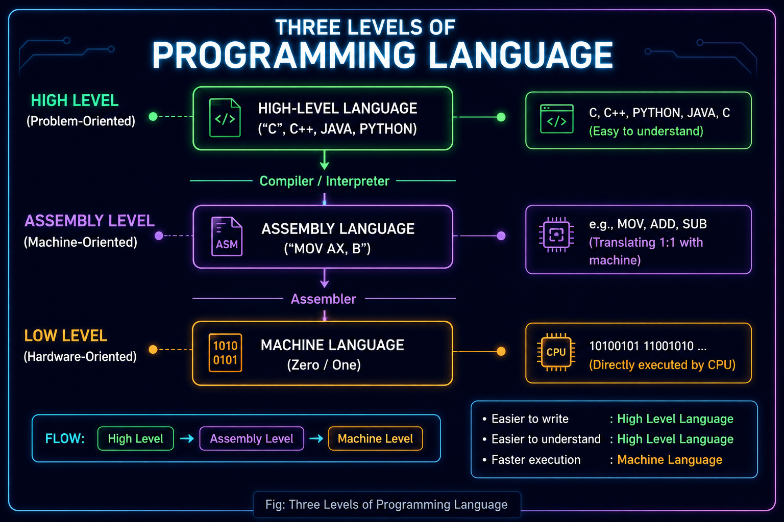
Language Levels → High-Level → Assembly (mnemonics) → Machine (binary)
Cycles → Instruction Cycle (Fetch-Decode-Execute-Store) built from Machine Cycles, built from Bus Cycles
Addressing Modes → Immediate (fastest) → Register → Direct → Indirect (slowest, most flexible)
Operations → Data Transfer, Arithmetic, Logical, Control Transfer, I/O
Instruction Types → Zero/One/Two/Three-address; Format = Opcode + Operand field(s)
1. Levels of Programming Languages
📖 Why "Levels"? Programming languages are organized in layers based on how close they are to the hardware (low-level) vs how close they are to human language (high-level).
💻 The Levels of Programming Language
| Level | Readability | Translator Needed | Example |
|---|
| High-Level Language | Human-friendly | Compiler/Interpreter | Python, Java, C++ |
| Assembly Language | Symbolic (mnemonics) | Assembler | MOV, ADD, SUB, JMP |
| Machine Language | Pure binary (0s/1s) | None — directly executed | 01001011... |
💡 Exam Tip: Machine language is machine-DEPENDENT (different for every CPU architecture); high-level languages are largely machine-INDEPENDENT (portable) — this is a common 2-mark differentiator.
2. Assembly Language Instructions
📖 Assembly Language: A low-level language that uses short, symbolic mnemonics (like ADD, MOV, SUB) instead of raw binary — each assembly instruction maps almost 1-to-1 to a single machine instruction.
| Mnemonic | Meaning | Example |
|---|
MOV | Move data between registers/memory | MOV AX, BX |
ADD / SUB | Arithmetic addition/subtraction | ADD AX, 5 |
LOAD / STORE | Load from memory / store to memory | LOAD R1, [200] |
JMP | Unconditional jump to an address | JMP 300 |
CMP | Compare two operands (sets flags) | CMP AX, BX |
JZ / JNZ | Jump if Zero flag set / not set | JZ 500 |
Assembler — The Translator:
An Assembler converts assembly language source code into machine code (object code) that the CPU can directly execute. Unlike a compiler, translation is nearly one-to-one — each assembly line usually becomes one machine instruction.
💡 Exam Tip: Assembly language is machine-dependent (each CPU family — Intel x86, ARM — has its own mnemonic set), which is why it's not portable across different processor architectures.
3. Machine Instructions — Machine Cycle and Bus Cycle
📖 Machine Instruction: The actual binary code that the CPU's hardware directly understands and executes — every assembly instruction is translated into one or more machine instructions.
Machine Cycle:
Fetch
→
Decode
→
Execute
→
Store
Fig: One Complete Machine Cycle (repeats for every instruction)
Machine Cycle = the time taken for the CPU to fetch ONE instruction from memory and execute it completely. Every instruction takes at least one machine cycle (complex instructions may take several).
Bus Cycle:
📖 Bus Cycle: The time taken to complete ONE data transfer over the system bus (e.g. one memory read or one memory write). A single machine cycle is usually made up of multiple bus cycles.
| Feature | Machine Cycle | Bus Cycle |
|---|
| Scope | One full instruction's execution | One single bus transfer (read/write) |
| Made of | Multiple bus cycles | Multiple clock cycles |
| Example | Fetch + Decode + Execute + Store | Just the "Fetch operand from memory" step |
💡 Exam Tip: Think of it as nested cycles: Clock Cycle (smallest) → Bus Cycle (a few clock cycles for one transfer) → Machine Cycle (a few bus cycles for one full instruction).
4. Addressing Modes
📖 Addressing Mode: The technique used to specify WHERE the operand (data) for an instruction is located — directly in the instruction, in a register, or in memory (possibly via an address stored elsewhere).
| Mode | How Operand is Found | Example |
|---|
| Immediate | Operand is part of the instruction itself | MOV AX, 5 → 5 is used directly |
| Direct | Instruction contains the memory address of the operand | MOV AX, [200] → read memory location 200 |
| Indirect | Instruction contains the address of a location that holds the address of the operand | MOV AX, [[200]] → address stored at 200 points to actual data |
| Register | Operand is inside a CPU register | MOV AX, BX → operand is in register BX |
| Register Indirect | Register holds the address of the operand (in memory) | MOV AX, [BX] |
| Indexed | Address = Base Address + Index Register value | Used for accessing array elements |
| Relative | Address = PC (Program Counter) + Offset | Used for branch/jump instructions |
| Mode | Speed | Flexibility |
|---|
| Immediate | ⚡ Fastest (no memory access) | Low |
| Register | ⚡ Very Fast | Medium |
| Direct | Medium (1 memory access) | Medium |
| Indirect | 🐢 Slowest (2 memory accesses) | High |
💡 Exam Tip: More memory references = slower but more flexible. Immediate mode never touches memory for the operand (fastest); Indirect mode touches memory twice (once to get the address, once to get the data).
Worked Example — Relative Addressing Mode:
Effective Address = PC (Program Counter) + Offset
💡 PYQ-Style Example: Given PC = 3000H and Offset = +005AH, find the Effective Address.
Effective Address = PC + Offset
= 3000H + 005AH
= 305AH
Role in branching: Relative addressing is heavily used in conditional/unconditional JUMP and BRANCH instructions — instead of storing a full absolute target address, the instruction stores a small offset relative to the CURRENT PC. This makes branch instructions shorter (fewer bits needed) and the code position-independent (works correctly even if the program is loaded at a different memory location).
💡 Exam Tip: Relative addressing offsets can be POSITIVE (branch forward) or NEGATIVE (branch backward, e.g. for loops) — always check the sign given in the question before adding.
5. Instruction Cycle & Types of Operations
Instruction Cycle:
📖 Instruction Cycle: The complete sequence of steps the CPU follows to fetch, decode, and execute ONE instruction — repeats continuously as long as the program runs.
1. Fetch
→
2. Decode
→
3. Fetch Operands
→
4. Execute
→
5. Store Result
Fig: The 5-Step Instruction Cycle
| Step | What Happens |
|---|
| 1. Fetch | Instruction fetched from memory (address given by PC), stored in IR; PC incremented |
| 2. Decode | Control Unit interprets the opcode — determines what operation to perform |
| 3. Fetch Operands | Any required data operands are fetched from registers/memory |
| 4. Execute | ALU or Control Unit performs the actual operation |
| 5. Store Result | Result written back to a register or memory location |
Types of Operations (what instructions can do):
| Category | Examples |
|---|
| Data Transfer | MOV, LOAD, STORE — move data between registers/memory |
| Arithmetic | ADD, SUB, MUL, DIV, INC, DEC |
| Logical | AND, OR, NOT, XOR, shift/rotate operations |
| Control Transfer | JMP, CALL, RET, conditional jumps (JZ, JNZ) — alter the flow of execution |
| Input/Output | IN, OUT — transfer data to/from I/O devices |
💡 Exam Tip: Fetch and Decode happen for EVERY instruction identically — it's only the Execute step that differs based on the opcode. This is why the Fetch-Decode part is called the "instruction cycle overhead."
6. Types of Instructions & Instruction Format
Types of Instructions (by Address Field Count):
📖 Classification: Instructions are classified by how many memory addresses/operands they explicitly reference — this affects instruction length and how many memory accesses are needed.
| Type | Format | Example: C = A + B |
|---|
| Zero-Address | Uses a stack; no operand addresses | PUSH A, PUSH B, ADD, POP C |
| One-Address | Uses Accumulator implicitly as 2nd operand | LOAD A, ADD B, STORE C |
| Two-Address | One operand doubles as destination | MOV R1, A, ADD R1, B, MOV C, R1 |
| Three-Address | Separate source(s) and destination | ADD C, A, B |
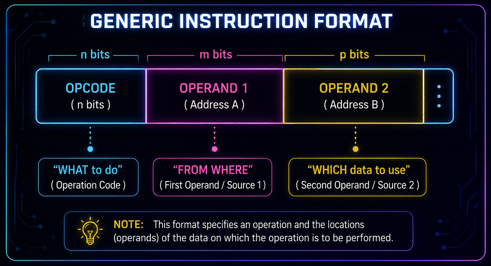
Instruction Format:
📖 Instruction Format: The layout describing how bits within a machine instruction are divided into fields — typically an Opcode field and one or more Operand/Address fields.
🧩 Generic Instruction Format
| Field | Purpose |
|---|
| Opcode (Operation Code) | Specifies WHICH operation to perform (ADD, SUB, MOV...) |
| Operand / Address Field(s) | Specifies WHERE the data is (register, memory address, or immediate value) |
| Mode Field | Specifies the addressing mode used to interpret the operand field |
💡 Exam Tip: Zero-address (stack-based) needs NO address fields at all but MORE instructions overall; Three-address is the opposite — fewer instructions but each is longer/bigger. This trade-off (instruction count vs instruction size) is a favourite 5-mark discussion question.
📚
Self-Study Topics
Self-Study Topics 📚 Extra Reading
📌 Note: These topics are listed as Self-Study in the syllabus — good to know for a well-rounded understanding, and occasionally asked. Read after finishing the core chapters above.
A. BCD and ASCII Data Representation:
BCD (Binary Coded Decimal): Each decimal digit (0-9) is represented separately using 4 binary bits. Example: 25 in BCD = 0010 0101 (NOT the same as plain binary 25 = 11001).
ASCII (American Standard Code for Information Interchange): A 7-bit (or 8-bit extended) code that represents each character (letters, digits, symbols) as a unique number. Example: 'A' = 65 = 01000001.
💡 Key Point: BCD wastes some bit patterns (4 bits can represent 0-15, but BCD only uses 0-9) — this makes BCD arithmetic slightly less efficient than pure binary, but easier to convert directly to/from decimal for display.
B. Little Endian vs Big Endian Memory Addressing:
📖 Endianness: The order in which bytes of a multi-byte value (like a 32-bit integer) are stored in memory.
Value: 0x12345678 stored starting at address 1000
BIG ENDIAN (most significant byte first):
Address: 1000 1001 1002 1003
Byte: 12 34 56 78
LITTLE ENDIAN (least significant byte first):
Address: 1000 1001 1002 1003
Byte: 78 56 34 12
Fig: Big Endian vs Little Endian Byte Ordering
| Type | Rule | Used By |
|---|
| Big Endian | Most significant byte stored at the LOWEST address | Network protocols, older Motorola/SPARC processors |
| Little Endian | Least significant byte stored at the LOWEST address | Intel x86, most modern desktop CPUs |
C. Instruction Pipelining (Introduction):
📖 Instruction Pipelining: A technique where multiple instructions are overlapped in execution — while one instruction is being executed, the next is being decoded, and the one after that is being fetched — like an assembly line.
Without Pipelining (one instruction fully finishes before next starts):
I1: [Fetch][Decode][Execute]
I2: [Fetch][Decode][Execute]
With Pipelining (stages overlap):
I1: [Fetch][Decode][Execute]
I2: [Fetch][Decode][Execute]
I3: [Fetch][Decode][Execute]
Fig: Pipelining Overlaps Instruction Stages
✅ Advantage: Significantly increases instruction throughput (more instructions completed per unit time) without needing a faster clock.
💡 Preview: Pipelining is covered in much more depth in Unit 3 (Pipeline Processing) — this is just an early introduction to the concept.
⚡
Ready for Exam?
Sab padh liya? Ab Quick Revision karo — formulas, key points aur common mistakes ek jagah!
Quick Revision Karo →
⚡
Quick Revision — Last Minute Exam Prep!
📌 How to Use: Read this 5-10 minutes before exam. Contains all important points in condensed form. Focus on tables, comparisons, and key formulas!
🖥️ Chapter 1.1 — Basic Functional Units
📖 5 Functional Units:
Input → Memory → CPU (ALU + Control Unit + Registers) → Output
💡 CPU = ALU + Control Unit + Registers — a key definition to remember.
🔑 Registers Cheat Sheet:
PC → address of NEXT instruction
IR → CURRENT instruction (being executed)
MAR → address being accessed right now
MDR → data going to/from memory
AC → holds arithmetic result
SP → top of stack
Trick: PC vs MAR confusion — PC is always the NEXT address; MAR is whatever address is CURRENTLY on the bus (could be data too).
BUS FORMULAS:
Max Memory = 2^(address bus width)
Address Lines needed = log₂(memory size)
Quick Numerical Recall:
1 MB = 2²⁰ → 20 address lines
4096 locations = 2¹² → 12 address lines
3 Buses:
Address (one-way, WHERE)
Data (two-way, WHAT)
Control (two-way, signals)
✅ Memory-Mapped vs Isolated I/O (5M-style):
Memory-Mapped → I/O shares memory's address space, same instructions (MOV/LOAD) work — simpler, but eats into memory space.
Isolated → I/O has its OWN separate address space, needs special instructions (IN/OUT) — Intel x86 uses this.
| Topic | Key Formula/Fact | Trick |
|---|
| Functional Units | Input, Memory, ALU, CU, Output | CPU = ALU+CU+Reg |
| Address Bus | 2ⁿ locations addressable | One-way, WHERE |
| Data Bus | Width = bits moved/cycle | Two-way, WHAT |
| Memory-Mapped I/O | Shared address space | Generic instructions |
🔢 Chapter 1.2 — Data Representation
📖 2's Complement (Key Concept):
Negative = flip all bits (1's complement) + 1.
Why preferred: only ONE zero, subtraction=addition (same adder circuit), no end-around carry.
Range (n-bit): −2ⁿ⁻¹ to +(2ⁿ⁻¹−1) → one EXTRA negative number vs signed magnitude.
🔑 Quick Convert Recipe (e.g. −45 in 8-bit):
1. Write +45 in binary → 0010 1101
2. Flip ALL bits (1's comp) → 1101 0010
3. Add 1 (2's comp) → 1101 0011
Verify: flip+1 again should give back +45.
IEEE 754 FORMAT:
Single (32-bit):
1 Sign | 8 Exponent (bias 127) | 23 Mantissa
Double (64-bit):
1 Sign | 11 Exponent (bias 1023) | 52 Mantissa
Value Formula:
(−1)^S × 1.Mantissa × 2^(Exp−Bias)
Quick Recall (10.25 example):
1010.01 → normalize → 1.01001×2³
→ biased exponent = 130 = 10000010
→ Final: 0 | 10000010 | 01001000000000000000000
⚠️ Overflow Rule (IMP!):
SAME sign + SAME sign = OPPOSITE sign result → Overflow!
(+)+(−) → overflow NEVER happens.
e.g. 4-bit: 0101(+5)+0100(+4)=1001(reads as −7) → Overflow!
✖️ Booth's Algorithm Rule (5M-style — draw the table!):
Check (Q₀, Q₋₁):
00/11 → just Shift Right (ASR)
10 → A = A − M, then Shift
01 → A = A + M, then Shift
Quick Recall: 7×3 example → 4 cycles → final A:Q = 0001 0101 = 21 ✓
| Topic | Key Formula/Fact | Trick |
|---|
| 2's Complement | 1's comp + 1 | One zero, easy subtract |
| Range (n-bit) | −2ⁿ⁻¹ to +(2ⁿ⁻¹−1) | One extra negative |
| IEEE 754 Single | 1+8+23 bits, bias 127 | Hidden "1." not stored |
| Overflow | same-sign in → opp-sign out | (+)+(−) never overflows |
| Booth's Algorithm | n+1 cycles for n-bit | 00/11 nop, 10 sub, 01 add |
⚙️ Chapter 1.3 — Instruction Set Architectures
🔑 Language Levels:
High-Level (Compiler) → Assembly (Assembler, mnemonics like MOV/ADD) → Machine (pure binary, direct execute)
Trick: Machine language = hardware-dependent; High-level = mostly portable.
📖 Instruction Cycle (IMP!):
Fetch → Decode → Fetch Operands → Execute → Store Result
Machine Cycle = time for ONE full instruction.
Bus Cycle = time for ONE bus transfer.
Machine Cycle is made of multiple Bus Cycles.
ADDRESSING MODES — Speed Order (5M-style):
Immediate (fastest, 0 mem access)
→ Register
→ Direct (1 mem access)
→ Indirect (slowest, 2 mem accesses)
Immediate = operand IN instruction
Direct = address IN instruction
Indirect = address-OF-address IN instruction
✅ Instruction Types by Address Count:
Zero-Address → Stack (PUSH/POP/ADD), no operand fields
One-Address → Accumulator implied (LOAD A, ADD B, STORE C)
Two-Address → ADD R1, B (one operand = destination too)
Three-Address → ADD C, A, B (separate source & destination)
Trade-off: fewer address fields = more instructions needed but each instruction is shorter.
📦 Instruction Format: Opcode field (WHAT to do) + Operand/Address field(s) (WHICH data) + Mode field (HOW to interpret operand).
| Topic | Key Formula/Fact | Trick |
|---|
| Language Levels | High→Assembly→Machine | Compiler→Assembler→direct |
| Instruction Cycle | Fetch-Decode-Execute-Store | 5 steps, always in order |
| Addressing Modes | Immediate fastest, Indirect slowest | More mem access = slower |
| Instruction Types | Zero/One/Two/Three-address | Stack→Acc→2addr→3addr |
📚 Self-Study — Quick Recall Extra
BCD: each decimal digit = 4 bits separately (25 → 0010 0101, NOT plain binary 11001).
ASCII: 7/8-bit code per character ('A' = 65 = 01000001).
Endianness:
Big Endian = MSB at LOWEST address (network, old Motorola)
Little Endian = LSB at LOWEST address (Intel x86, most modern CPUs)
Pipelining: overlaps Fetch/Decode/Execute of consecutive instructions — like an assembly line — increases throughput without a faster clock. (Full depth in Unit 3.)
⚠️ Common Exam Mistakes
❌ Confusing PC (next instruction) with MAR (current address being accessed)
❌ Forgetting 2's complement has only ONE extra negative number, not symmetric range
❌ Wrong overflow rule — forgetting it only happens with SAME-sign operands
❌ Mixing up Big Endian (MSB at lowest address) vs Little Endian (LSB at lowest address)
❌ In Booth's Algorithm, forgetting to check the PREVIOUS bit (Qₙ₊₁) along with current bit
❌ Not showing the hidden "1." bit explanation in IEEE 754 questions
✅ Pre-Exam Checklist
☑ 5 functional units + CPU components
☑ All registers — PC, IR, MAR, MDR, AC, SP
☑ 3 buses — direction & purpose of each
☑ Memory-mapped vs Isolated I/O
☑ 2's complement — why preferred, range formula
☑ IEEE 754 single/double precision format
☑ Overflow detection rule
☑ Booth's Algorithm — full cycle table practice
☑ Array multiplier (shift-add) method
☑ 7 addressing modes with examples
☑ Instruction cycle — 5 steps in order
☑ Zero/One/Two/Three-address instruction formats
☑ (Self-Study) BCD/ASCII, Endianness, Pipelining basics
🎯 Exam Strategy
2 Mark Questions:
• Direct definition + 1 example. Time: 3-4 minutes.
• "Differentiate" → always draw a 2-column table.
5 Mark Questions:
• Definition + Diagram/Table + Worked Numerical. Time: 7-8 minutes.
• Numericals (2's complement, IEEE 754, Booth's) — show EVERY step, don't skip to the answer.
Marks-saving tip:
Even if the full numerical isn't finished, writing the correct rule/formula and the first 1-2 steps earns partial marks!
🌟 All the Best!
COA is heavy on numericals — 2's complement, IEEE 754, Booth's Algorithm. Practice these by hand, step by step, not just once — muscle memory matters here. Tables और diagrams yaad karo, aur tu ready hai! 💪🖥️
📄
Previous Year Questions
📌 Source: Mid Semester Test-1 (MST-1), Academic Year 2025-2026 — Unit 1 only. Maximum Marks: 20, Time: 1 Hour.
Section A (5 × 2 = 10 marks)
2M
MST-1
List the differences between address bus and data bus.
▼
Address Bus: Unidirectional (CPU → Memory/IO only), carries the memory ADDRESS the CPU wants to access, width determines max addressable memory (2ⁿ locations).
Data Bus: Bidirectional (data flows both ways), carries the actual DATA being transferred, width determines how many bits move per cycle.
See Chapter 1.1, Section 3 for the full comparison table and diagram.
2M
MST-1
Define primary memory and secondary memory, and list the differences between them.
▼
Primary Memory: Memory directly accessible by the CPU — volatile, very fast, limited size (e.g. RAM, Cache, Registers).
Secondary Memory: Memory NOT directly accessible by the CPU — data must be loaded into primary memory first. Non-volatile, slower, much larger capacity (e.g. Hard Disk, SSD, DVD).
Key differences: CPU access (direct vs indirect), volatility, speed, capacity, cost — full table in Chapter 1.1, Section 4.
2M
MST-1
Illustrate the stages involved in an instruction cycle.
▼
The 5 stages, in order: 1. Fetch (get instruction from memory, PC points to it) → 2. Decode (Control Unit interprets the opcode) → 3. Fetch Operands (get required data) → 4. Execute (ALU/CU performs the operation) → 5. Store Result (write back to register/memory).
See Chapter 1.3, Section 5 for the full diagram and table.
2M
MST-1
Describe the role of the program counter (PC) in instruction execution.
▼
The Program Counter (PC) holds the ADDRESS of the NEXT instruction to be fetched — not the current one. During the fetch stage, the CPU reads the instruction at the address in PC, and PC is then automatically incremented to point to the following instruction, keeping execution flowing sequentially (unless a jump/branch instruction changes it directly).
2M
MST-1
List any two types of instructions based on operation type.
▼
Any two of: Data Transfer (MOV, LOAD, STORE), Arithmetic (ADD, SUB, MUL), Logical (AND, OR, NOT), Control Transfer (JMP, CALL, RET), Input/Output (IN, OUT). Full list in Chapter 1.3, Section 5.
Section B (2 × 5 = 10 marks)
5M
MST-1
Convert the decimal number 58.375 into its normalized IEEE 754 single-precision (32-bit) floating-point representation. Clearly explain the steps involved in determining the sign bit, exponent and mantissa.
▼
Step 1 — Convert integer part 58 to binary:
58 = 32 + 16 + 8 + 2 = 111010
Step 2 — Convert fractional part 0.375 to binary:
0.375 × 2 = 0.75 → bit 0
0.75 × 2 = 1.5 → bit 1 (carry, remainder 0.5)
0.5 × 2 = 1.0 → bit 1 (remainder 0, stop)
0.375 = 0.011
Step 3 — Combine:
58.375 = 111010.011
Step 4 — Normalize to 1.xxxx × 2^e form:
Move the binary point 5 places to the LEFT (so only one "1" remains before the point):
111010.011 = 1.11010011 × 2⁵
So the exponent (unbiased) = 5
Step 5 — Determine the Sign bit:
The number is positive → Sign = 0
Step 6 — Calculate the Biased Exponent:
Single precision bias = 127
Biased Exponent = 5 + 127 = 132
132 in binary (8 bits) = 10000100
Step 7 — Determine the Mantissa:
Take the bits AFTER the leading "1." (which is never stored — the "hidden bit"): 11010011
Pad with zeros to fill all 23 mantissa bits:
Mantissa = 11010011000000000000000
Final IEEE 754 Representation:
0 | 10000100 | 11010011000000000000000
(Sign | Exponent (8 bits) | Mantissa (23 bits))
5M
MST-1
Break down the relative addressing mode by analyzing a given program counter value of 3000H and an offset of +005AH. Calculate the effective address and evaluate its role in supporting branching operations.
▼
What is Relative Addressing Mode?
In relative addressing, the effective (actual) memory address of the operand is calculated by ADDING an offset value to the current contents of the Program Counter (PC) — rather than storing a full absolute address directly in the instruction.
Formula:
Effective Address = PC + Offset
Given Values:
PC = 3000H
Offset = +005AH
Step-by-step Calculation (hexadecimal addition):
3000H
+ 005AH
────────
305AH
(Units: 0+A=A, Tens: 0+5=5, Hundreds: 0+0=0, Thousands: 3+0=3)
Effective Address = 305AH
Role in Branching Operations:
1. Shorter instructions: Only a small offset needs to be stored in the instruction (instead of a full absolute address), reducing instruction size/bits needed.
2. Position-independent code: Since the address is calculated RELATIVE to the current PC, the same program can be loaded at different memory locations and still branch correctly — very useful for relocatable code and loops.
3. Bidirectional branching: The offset can be positive (branch FORWARD, skipping ahead) or negative (branch BACKWARD, e.g. looping back to repeat instructions) — this flexibility is exactly what conditional/unconditional JUMP instructions rely on.